
|
"On Edge" DLX Computer Project |
Downloads Available:
The main objective for the project was to produce a fully pipelined DLX processor. This objective was broken into many smaller pieces for simplification. The first milestone was to produce a machine language version of the bubble sort algorithm, since the processor can only read machine code. Once this was accomplished, the next milestone was to produce a block diagram of the architecture. The following milestone was to write a small program that would take the machine code from the first milestone and import it into the source code for the processor. A test program was then written in Assembly language, converted into machine language, and inserted into the processor. The next milestone was to successfully simulate an ADD instruction. Once this was completed, the full bubble sort program was successfully simulated. After simulation, the last milestone was to load the source code onto a programmable gate array and successfully emulate the program on the chip.
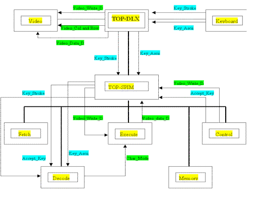
The next step was to enhance the DLX processor with two more modules. To serve that purpose, another level was added to the fully pipelined DLX processor. This level consisted of three different modules. The central module was TOP-DLX, which was responsible for assembling the TOP-SPIM module (written in the first part of the project) with the two additional modules. The first of those modules was a keyboard component. The keyboard module is an acquisition module for a PS/2 Keyboard.
Along with the keyboard, there was the addition of a video module, in which memory is allocated in the form of RAM.
Instruction set
Before the program could be written, an
instruction set had to be defined. This set was specified to be a
subset of the DLX instruction set. Once the instruction set was
defined, the instruction format was created. Figure 1 is a summary of the instructions used in the bubble
sort program. It resembles the format of the DLX architecture.
ADD
ADD: DEF OPSPECIAL,BLANK5,BLANK5,BLANK5,B#00000,FADD
OPSPECIAL: EQU Q#00
ADD: EQU Q#40
Ex : ADD R1, R2,
R3
Adds R2 and R3 in R1
0
5
6
10
11
15
16
20
21
25
26
31
| 00 | reg dest=R1 | operand=R2 | operand=R3 | 00000 | 20 |
ADDI
ADDI: DEF OPADDI,BLANK5,BLANK5,BLANK16
OPADDI: EQU Q#06
Ex : ADDI R1, R2, H#0003
Adds R2 and value at H#0003 in R1
0
5
6
10
11
15
16
31
| 06 | reg dest=R1 | reg src=R2 | Immediate |
LW and SW
LW: DEF OPLW,BLANK5,BLANK5,BLANK16
SW: DEF OPSW,BLANK5,BLANK5,BLANK16
OPLW: EQU Q#43
OPSW: EQU Q#53
EX : LW R1, R2, H#0000
0
5
6
10
11
15
16
31
| 43 | reg dest=R1 | reg src=R2 | immediate |
BEQZ and BNEZ
BEQZ: DEF OPBEQZ,BLANK5,NULL5,BLANK16
BNEZ: DEF OPBNEZ,BLANK5,NULL5,BLANK16
OPBEQZ: EQU Q#04
OPBNEZ: EQU Q#05
Ex : BEQZ R2, 06
Jumps to
instruction 06 if value in R2 = 0
0
5
6
10
11
15
16
31
| 04 | reg used=R2 | 00000 | instruction address |
J and JAL
J: DEF OPJ,26VB#00000000000000000000000000
JAL: DEF OPJAL,26VB#00000000000000000000000000
OPJ: EQU Q#02
OPJAL: EQU Q#03
Ex : J <value>
Unconditional jump to instruction <value>
0
5
6
31
| 02 | value |
JAL test
Jumps to
instruction labeled as test
0
5
6
31
| 03 | test |
JR
JR: DEF OPJR,BLANK5,NULL16,B#01000
OPJR: EQU Q#20
Ex: JR R1
0
5
6
10
11
26
31
| 20 | reg used=R1 | 0000000000000000 | 01000 |
SLL
SLL: DEF OPSPECIAL,BLANK5,BLANK5,BLANK5,BLANK5,FSLL
OPSPECIAL: EQU Q#00
FSLL: EQU Q#04
Ex : SLL R2
Shifts the value
in register 2 by 2, therefore multiplying by 4
0
5
6
10
11
26
31
| 00 | reg used=R2 | 0000000000000000 | 04 |
SLT
SLT: DEF OPSPECIAL,BLANK5,BLANK5,BLANK5,B#00000,FSLT
OPSPECIAL: EQU Q#00
FSLT: EQU Q#52
EX : SLT R3,R2,R1
Sets R3 to be zero if R2 is less than R1
0
5
6
10
11
15
16
20
21
25
26
31
| 00 | reg used=R3 | operand=R2 | operand=R3 | 00000 | 52 |
NOP
NOP: DEF OPADDI,BLANK5,BLANK5,BLANK16
OPNOP: EQU Q#77
0
5
6
10
11
15
16
31
| 77 | 00000 | 00000 | 0000000000000000 |
Figure 1. Summary of instruction formats used in
bubble sort
The addition of a video and keyboard module had repercussions on many stages of the program, including the instruction set. At first, there was a need for a more complete instruction set. However, only one more instruction was necessary, known as PutChar. Here is the format of this instruction as well as its usage:
0
5
6
10
11
15
16
23
24
31
| 54 | Char-Mode | Reg value | 0000000 | Immediate |
The instruction format is : OpCode, Blank5, Blank5, 00000000, Blank8
The format of the instruction is similar to other instructions so that forwarding is implemented the same way.
The Opcode is defined as 101100. The next 5
bits correspond to the selection of the type of outputs.
Char_Mode is a 5 bit signal that enables us to select the type.
(Only 2 bits are used at the moment, but more may be required
later on).
Bits 12 to 16 give the value of the register
that needs to be printed to the screen.
Types of outputs:
00 : In this case, the most significant hex digit of the register passed will be outputted to the screen. ( There is the assumption that we are displaying two hex numbers). 01 Now, the least least significant hex digits are selected, and outputted to the screen. 10 Used when there is a need to write a character passed by the compiler (at the assembly level). This would select the last 8 bits from the instruction. When the first 2 bits are ‘00’, the remaining 6 bits are the ascii code for the character that will be outputted. When ‘01’, this corresponds to the enter key, therefore there will be no output to the screen. When ‘10’, a ‘backspace’ key is passed, so there will be no output either. 11 This is never suppose to be passed, but assigning 00000000 to avoid powering up in an unknown state.
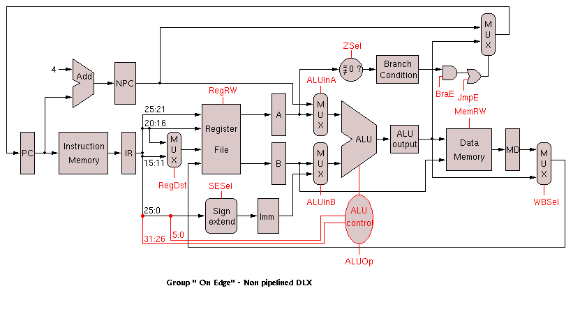
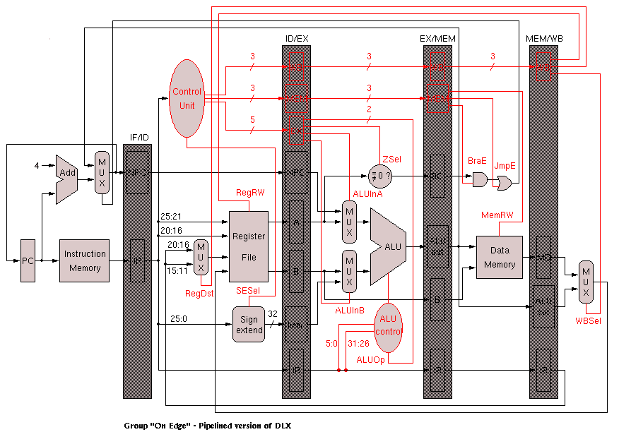
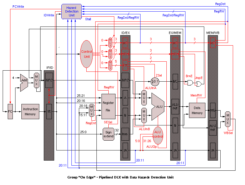
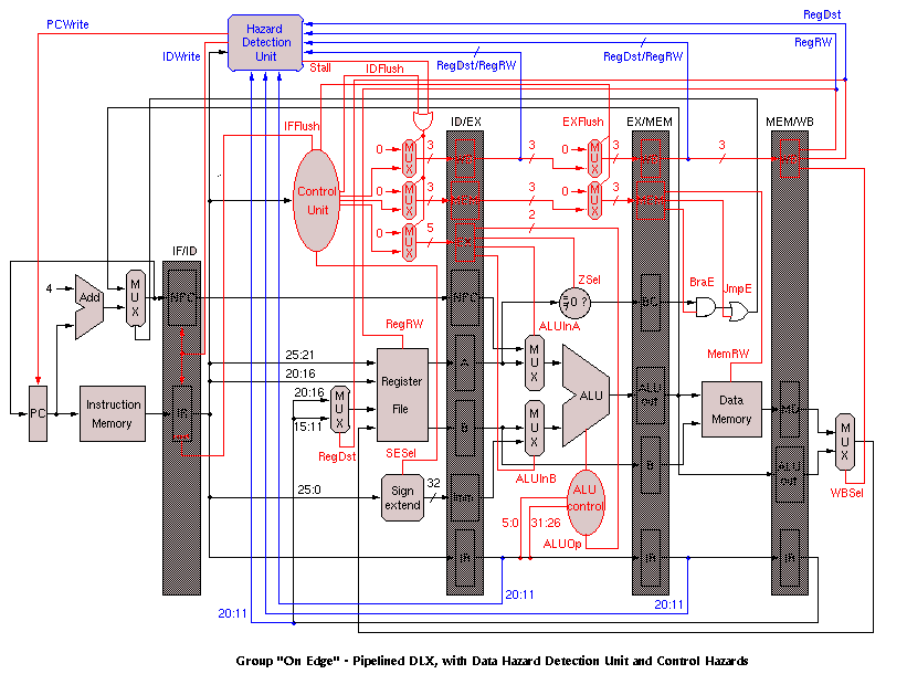
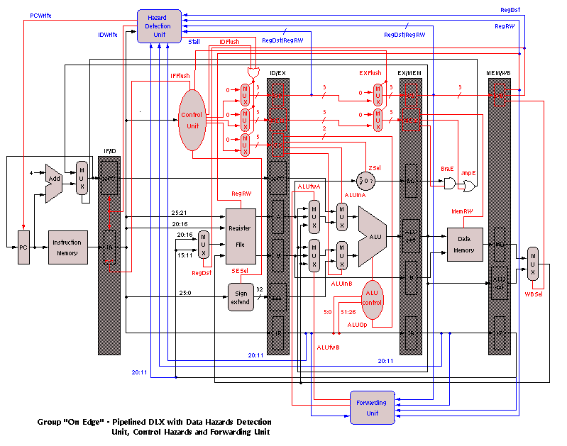
The next milestone was to draw a block diagram of the system based on the DLX diagrams in Patterson and Hennesey. This proved to be a vital part of the project. Due to the complexity of the final diagram, the schematic is provided in different stages. The first figure is the simplest version of the architecture, showing the processor as a single stage (non-pipelined) version. It shows the basic components that make up the processor, including the instruction memory, the register files, the ALU, and the data memory. The following block diagram shows the same processor broken into five stages. The control unit was also added to show the different control signals controlling the various units, such as the ALU and the data memory. The hazard detection unit was added to the decode unit and is responsible for determining whether possible hazards exist. Although hazard detection is one of the disadvantages to running a pipelined system, it is possible that a result is needed in an instruction register value that has not been written to the register yet. In this case, the hazard detection unit would, if possible, forward the correct value; otherwise, it would stall the pipeline long enough to avoid the problem. The last two diagrams are very similar, but the flushing signals added to the last block diagram shows which units had to be stalled when the forwarding unit could not resolve the hazard. This occurred in two instances: whenever the instruction is a branch, or whenever a LW instruction was followed by an instruction needing that value. For example, LW R5, R2, H0002 followed by ADD R1, R5, R6 would cause a hazard. In the case of the branch, the branch is not determined immediately. By the time it is determined, the next instruction has already been loaded into the processor. The control signals are responsible for flushing that instruction and correctly branching to the new instruction. Originally, the branch was determined in the execute stage of the pipeline; therefore, branch flushing would cause two instructions to be flushed from the pipeline. By calculating the branch address in the decode stage, only one instruction would have to be flushed. In the current implementation, the need for forwarding is determined in the decode stage; however, the forwarding values are not needed until later stages. Because the branch address is now calculated in the decode stage, it was necessary to provide forwarding for the branch and zero calculation in the decode module.
The hazard detection and forwarding units are also needed to prevent problems with the LW instruction. Because the value from the LW is not determined until the instruction reaches the data memory, the instruction following the LW must wait until the value has been loaded from memory. This requires a stall after the LW, which must be implemented by the compiler. Since this project did not include a compiler, it was inserted manually. This last block diagram represents the final version of the block diagram, which includes the forwarding unit. All result signals are routed back to the ALU in case they were needed for calculations.
With the addition of the keyboard and video modules, a third level was added to the DLX processor. The combination of these two modules with TOP-DLX enables the input of characters through the processor, and visualization of the characters on a screen. Here is a representation of the project with the three different levels.
Implementation
After the instruction set was defined, the
bubble program, which was given in the programming language C
(see Figure 2), had to be written in Assembly language.
Int v[111 102 14 –13 17 6 5 0];
Sort(int v[], int n)
{
int I, j;
for (I = 0; I < n ; I ++)
{
for (j = I – 1 ; j >= 0 && v[j]>v[j+1] ; j --)
{
swap(v,j);
}
}
}
Figure 2. C code for sort program
Using the example in "Computer Architecture A Quantitative Approach" by Patterson and Hennessy, the bubble sort program was written in Assembly language. In order to convert the assembly language file into machine language, a macro file and a meta-assembler program called TIM were used. The meta-assembler creates a machine language with instruction program counters using any assembly language source file.
It was then necessary to write a program that would convert the machine code produced by TIM into the instruction code for the processor. This was done using the Progress 4GL programming language. The "convmif.p" program converts the "sort.lst" file generated from TIM into an Altera formatted MIF (Memory Initialization File). The MIF was then used to initialize the ROM defined in the Instruction Fetch module. This program provided an easy way to write test programs, run them through the TIM meta-assembler, and convert them into MIF files for the Altera program.
This program provided the instruction set that was needed in the MIF format. All instructions starting with a ‘B’ are PutChar instructions, instructions that were added to test the functionality of the third level of the DLX processor. Here is the link for the instruct.mif file.
Using the instruction set for the bubble sort algorithm, the VHDL code was compiled and simulated.
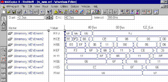
The waveform simulation shows that the memory locations 1-8 are initialized to 6F, 66, 0F, F3, 11, 06, 05 and 00 respectively. The intermediary clock cycles show the swapping of the memory locations. For example, after a number of clock cycles, 6F and 66 are swapped because 66 is smaller than 6F. Then 6F and 0E are swapped, followed by 66 and 0E. This algorithm was repeated until the numbers were sorted in memory in ascending order. Therefore, the final ordering of the number was as follows: "F3, 00, 05, 06, 0E, 11, 66, 6F", as the ouput to the screen shows.