
Using the Video on the Altera UP1 Board
|
Using the Video on the Altera UP1 Board |
The Altera UP1 board contains a VGA port which allows a possible resolution of 640x480 pixels using five output signals(red, green, blue, horizontal sync, and vertical sync). The VHDL module video.vhd supports a maximum of 40x16 characters using a character set where each letter is an 8x8 unit block. Each block unit consists of 16x16 pixels. (This was done by slowing down the clock used to determine the value of each pixel.) The clock used is the 25.175MHz clock on the UP1 board.
Character Set
Because the screen is constantly being refreshed, it was
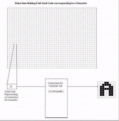
necessary to define a RAM to hold the characters being displayed
on the screen. Due to a limited amount of RAM, the screen was
mapped into 16 rows and 40 columns. (The VGA display used is
capable of displaying 30 rows; however, the FLEX 10K20 device is
unable to support the RAM required; therefore, it was limited to
the top 16 rows.) Each row-column combination is stored in a
video RAM(format_ram) as a 10-bit address where the RAM address
is defined as follows:
RAM Address <= row_address(3 downto 0) & column_address(5 downto 0);
Each RAM Address holds a 6-bit octal code which maps to a ROM(tiny_char_gen_rom) defining a subset of the Commodore 64 character set. A Memory Initialization File(vidram.mif) was used to define the contents of the video RAM. The character set ROM was initialized using a file called tcgrom.mif.
The character ROM would show the letter "A" as the following addresses.
The Letter "A"
010 : 00011000 ;
011 : 00111100 ;
012 : 01100110 ;
013 : 01111110 ;
014 : 01100110 ;
015 : 01100110 ;
016 : 01100110 ;
017 : 00000000 ;
The Commodore 64 character set used to display the characters was provided by Dr. James Hamblen. Due to limited RAM, only the capital letters and some numbers and symbols were provided. The table below shows the keyboard character followed by its octal address. For example, a space is represented by octal code 40. The repeated letters A-F were used to simplify the displaying of HEX values.
| A | 01 | B | 02 | C | 03 | D | 04 | E | 05 | F | 06 | G | 07 | H | 10 | I | 11 | ||||||||
| J | 12 | K | 13 | L | 14 | M | 15 | N | 16 | O | 17 | P | 20 | Q | 21 | R | 22 | ||||||||
| S | 23 | T | 24 | U | 25 | V | 26 | W | 27 | X | 30 | Y | 31 | Z | 32 | [ | 33 | ||||||||
| Down | 34 | ] | 35 | Up | 36 | Left | 37 | Space | 40 | ! | 41 | " | 42 | # | 43 | $ | 44 | ||||||||
| % | 45 | & | 46 | ' | 47 | ( | 50 | ) | 51 | * | 52 | + | 53 | , | 54 | - | 55 | ||||||||
| . | 56 | / | 57 | 0 | 60 | 1 | 61 | 2 | 62 | 3 | 63 | 4 | 64 | 5 | 65 | 6 | 66 | ||||||||
| 7 | 67 | 8 | 70 | 9 | 71 | A | 72 | B | 73 | C | 74 | D | 75 | E | 76 | F | 77 |
Video Refresh
The screen refresh process begins in the top left corner and
paints 1 pixel at a time from left to right. At the end of the
first column, the row increments and the column address is reset
to the first column. Each row is painted until all pixels have
been displayed. Once the entire screen has been painted, the
refresh process begins again.
Using the Video RAM Module
The video module included here expects that a higher module is
calling video. Many of the signals defined here are to be passed
from video out of the chip to the UP1 board.
entity video is
Generic(ADDR_WIDTH: integer := 12; DATA_WIDTH: integer := 1);
port(signal PB1, PB2, BrdClock, Clock : in std_logic;
signal LSB_a, LSB_b, LSB_c, LSB_d, LSB_e, LSB_f, LSB_g, LSB_dp,
MSB_a, MSB_b, MSB_c, MSB_d, MSB_e, MSB_f, MSB_g, MSB_dp : out std_logic;
signal Red,Green,Blue : out std_logic;
signal Horiz_sync,Vert_sync : out std_logic;
signal switch : in std_logic_vector(0 to 7);
signal DLX_Clock,Reset : out std_logic;
signal MSB_Dot,LSB_Dot : in std_logic;
signal MSB_Data,LSB_Data : in std_logic_vector(3 downto 0);
signal video_data : in std_logic_vector(5 downto 0);
signal video_row, video_col : in std_logic_vector(5 downto 0);
signal video_write : in std_logic);end video;
The UP1 boards needs the following signals defined in the ACF file in order to display the signals.
|BrdClock : INPUT_PIN = 91;
|Blue : OUTPUT_PIN = 238;
|Green : OUTPUT_PIN = 237;
|Horiz_Sync : OUTPUT_PIN = 240;
|Vert_Sync : OUTPUT_PIN = 239;
|Red : OUTPUT_PIN = 236;
If you wish to use the seven segment display, the Flex Switches, or the debounce buttones, you will need to define these additional pin assignments.
|MSB_dp : OUTPUT_PIN = 14;
|MSB_g : OUTPUT_PIN = 13;
|MSB_f : OUTPUT_PIN = 12;
|MSB_e : OUTPUT_PIN = 11;
|MSB_d : OUTPUT_PIN = 9;
|MSB_c : OUTPUT_PIN = 8;
|MSB_b : OUTPUT_PIN = 7;
|MSB_a : OUTPUT_PIN = 6;
|LSB_dp : OUTPUT_PIN = 25;
|LSB_g : OUTPUT_PIN = 24;
|LSB_f : OUTPUT_PIN = 23;
|LSB_e : OUTPUT_PIN = 21;
|LSB_d : OUTPUT_PIN = 20;
|LSB_c : OUTPUT_PIN = 19;
|LSB_b : OUTPUT_PIN = 18;
|LSB_a : OUTPUT_PIN = 17;
|Flex_switch_1 : INPUT_PIN = 41;
|Flex_switch_2 : INPUT_PIN = 40;
|Flex_switch_3 : INPUT_PIN = 39;
|Flex_switch_4 : INPUT_PIN = 38;
|Flex_switch_5 : INPUT_PIN = 36;
|Flex_switch_6 : INPUT_PIN = 35;
|Flex_switch_7 : INPUT_PIN = 34;
|Flex_switch_8 : INPUT_PIN = 33;
|PB1 : INPUT_PIN = 28;
|PB2 : INPUT_PIN = 29;
Populating Video RAM
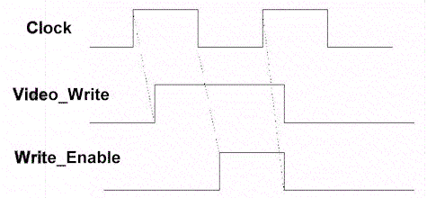
Due to set-up and hold times, it is necessary to pass two
separate clocks into the video module. The UP1 board
clock(brdclock) is used to produce a slower clock called
"Clock". The signal "Clock" is used to
generate a write enable signal when clock is '0' and video_write
is '1'. This provides enough time for the address lines(video_col
and video_row) and data line(video_data) to become stable.
Although both the column and row signals are defined as 6 bit vectors, the column signal should be between 0 and 40, and the row signal should be between 0 and 15. The data signal is a 6 bit signal which corresponds to the tiny character octal value listed above.